Real-Time Digital Filter for Ultrasonic NDT
🔍 Overview
Designed and implemented a high-speed real-time digital filtering system for Ultrasonic Non-Destructive Testing (NDT) applications.
The system processes ultrasonic signals using an FPGA-based FIR filter with dynamic coefficient control, enabling flexible filtering (LPF, HPF, BPF) based on user input.
🎯 Objective
- Process high-frequency ultrasonic signals in real time
- Implement dynamic digital filtering using FPGA
- Provide user-controlled filter configuration via GUI
- Ensure high signal integrity using optimized PCB design
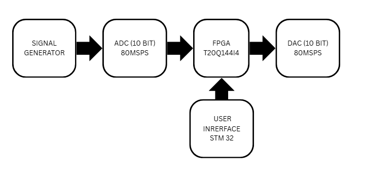
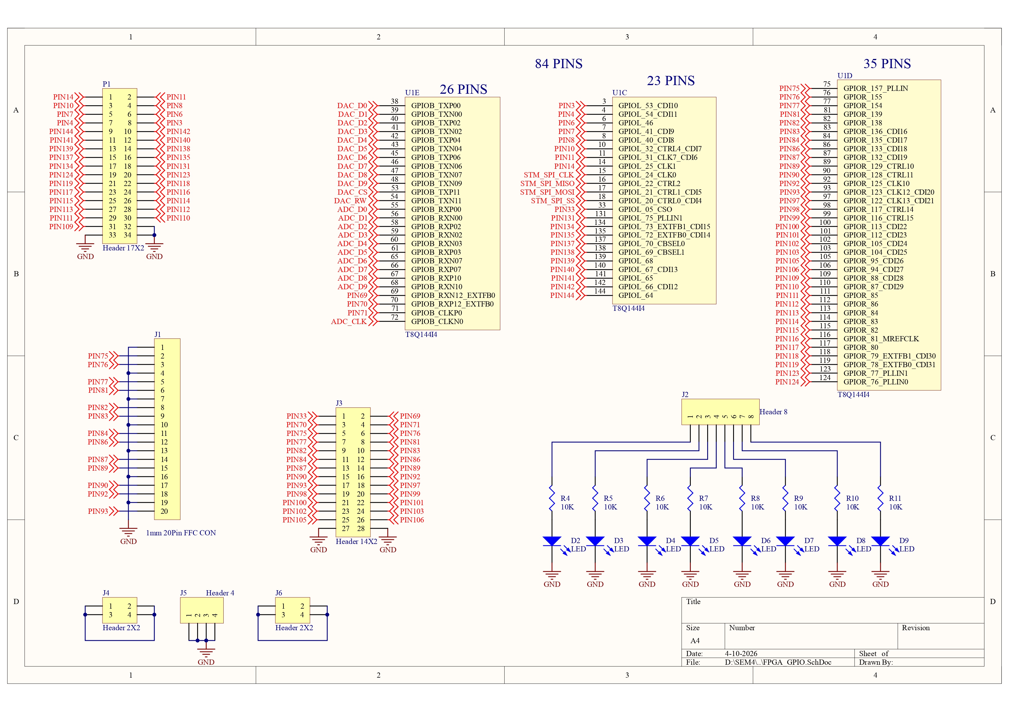
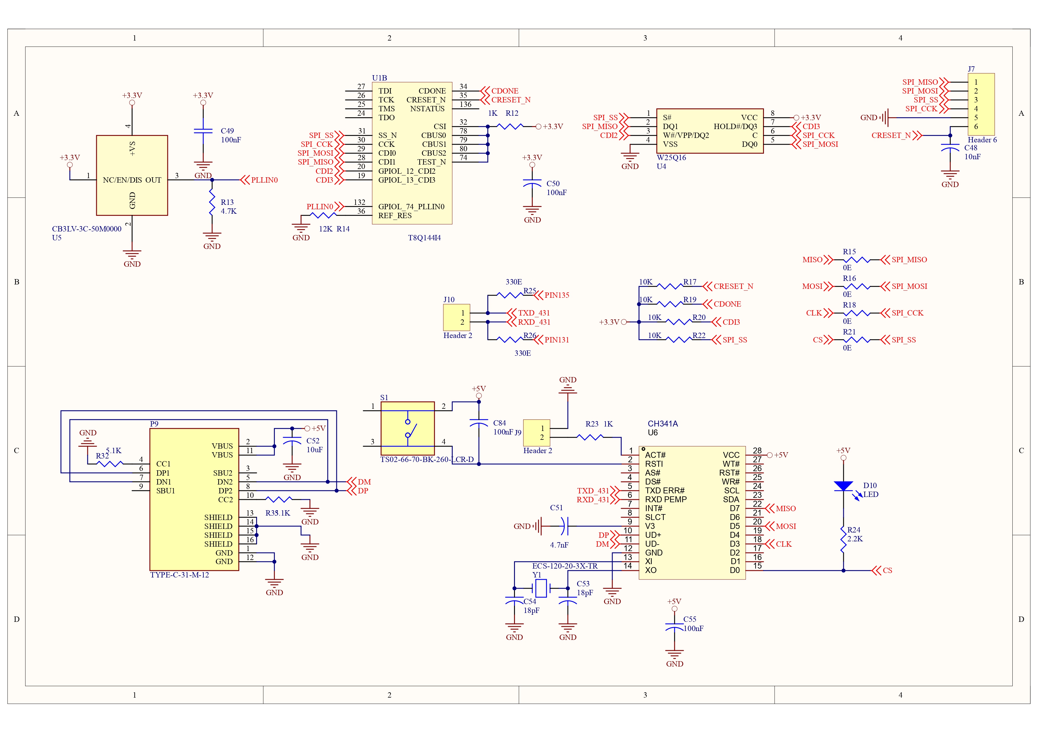
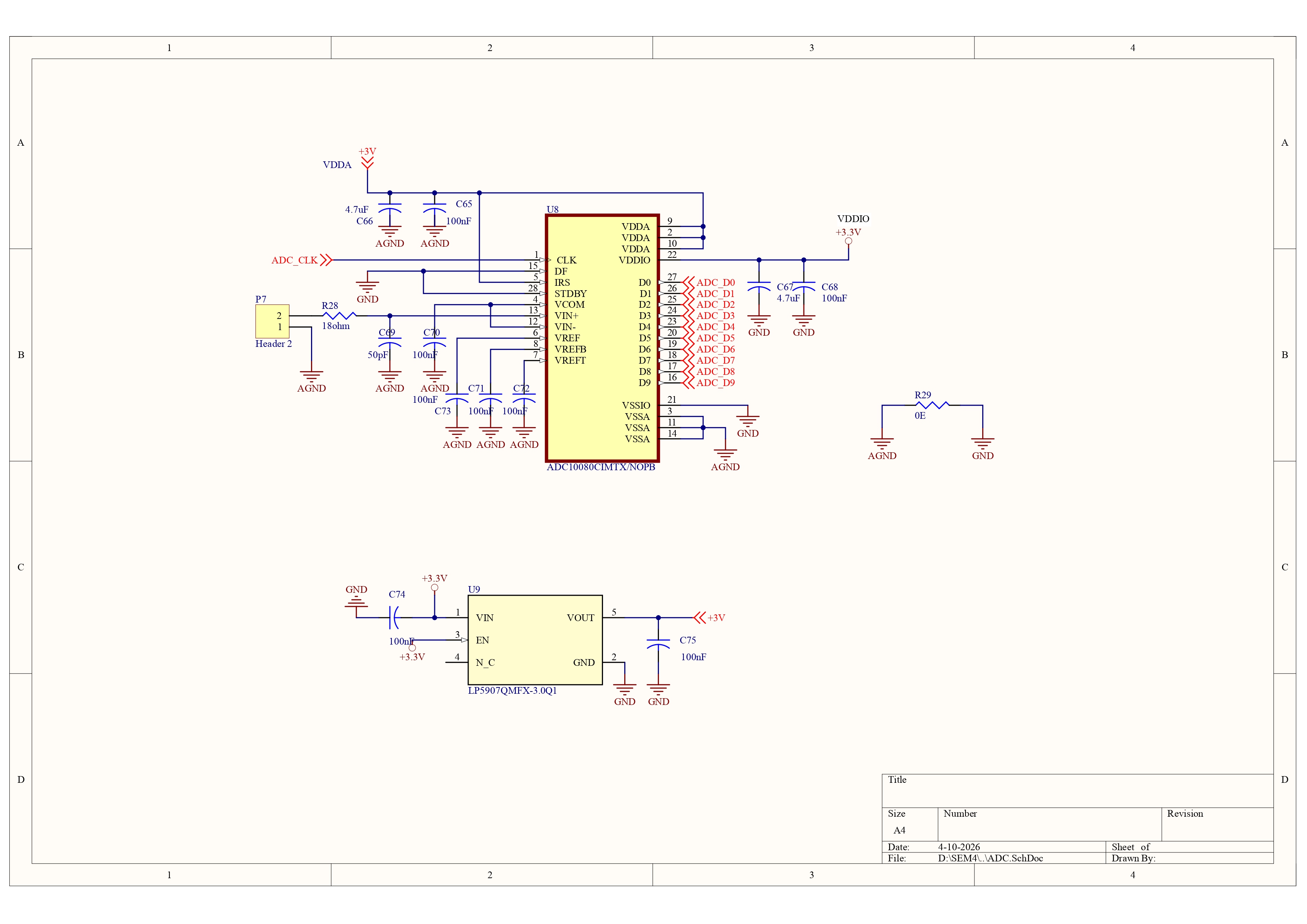
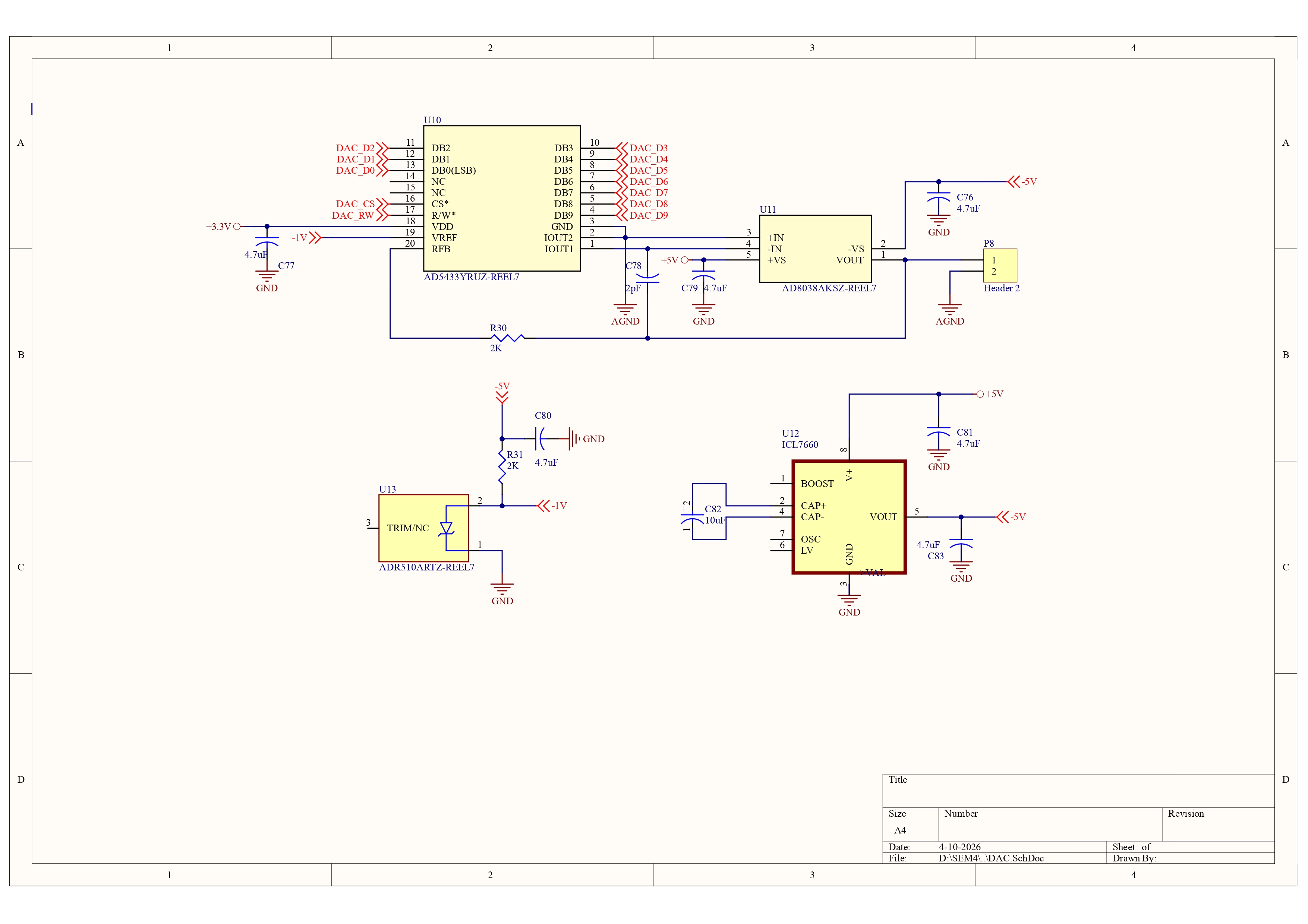
🧠 System Architecture
Ultrasonic Signal → ADC → FPGA (FIR Filter) → DAC → Output
↑
STM32 ↔ Python GUI
📐 Block Diagram
⚙️ Key Features
- Real-time FIR filtering on FPGA
- Dynamic filter selection (LPF, HPF, BPF)
- User input via Python-based GUI
- High-speed ADC and DAC integration
- Low-noise 4-layer PCB design
- SPI/UART communication between STM32 and FPGA
🧩 Hardware Components
🔹 Data Conversion
- ADC: ADC10080 (High-speed 10-bit ADC)
- DAC: AD5433 (High-speed DAC)
🔹 Processing Units
- FPGA: Cyclone 10 LP (T20Q144I4)
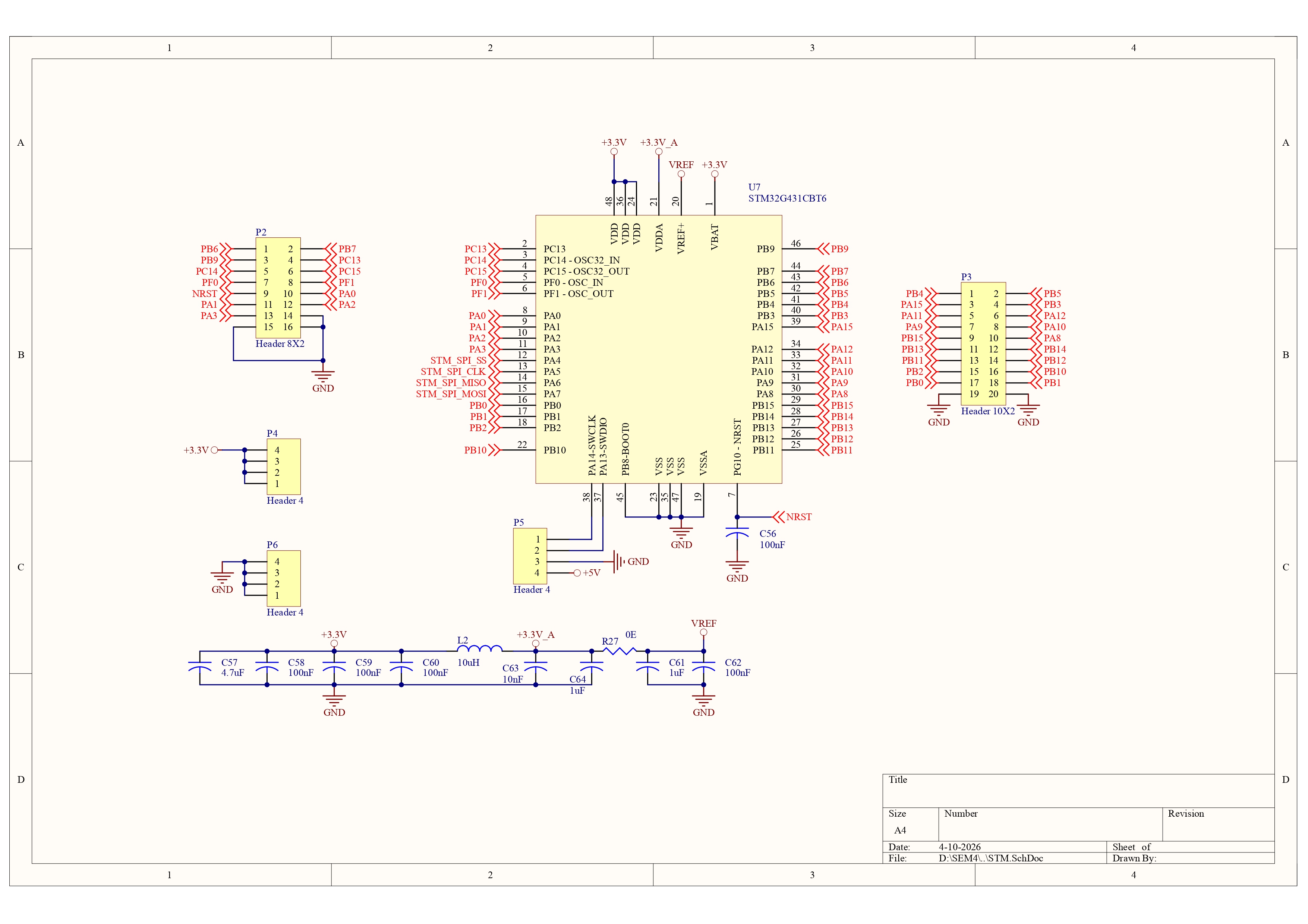
- Microcontroller: STM32G431CBT6
🔹 Supporting Hardware
- Analog front-end for ultrasonic signal conditioning
- Clock generation circuitry
- Power regulation modules
🛠 Tools & Software
- Verilog (FIR filter design)
- STM32CubeIDE (Embedded C)
- Python (GUI for user input)
- Efinity (FPGA synthesis)
- GTKWave (simulation)
- Altium Designer (PCB design)
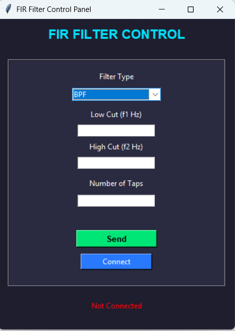
💻 GUI (User Interface)
- Developed a Python-based GUI for filter control
- User can select:
- Filter type (LPF / HPF / BPF)
- Cutoff frequency
- GUI sends parameters to STM32 via UART
 —
—
🔄 Working Principle
- Ultrasonic signal is captured and digitized using ADC10080
- Digital samples are fed into FPGA
- FIR filter processes the signal in real time
- STM32 computes filter coefficients based on user input
- Coefficients are sent to FPGA via SPI
- Filtered signal is converted back using DAC (AD5433)
🧮 FIR Filter Implementation
- Parallel MAC-based FIR architecture
- Coefficients stored in FPGA internal memory
- Fixed-point arithmetic for high-speed operation
- Pipeline stages used for timing optimization
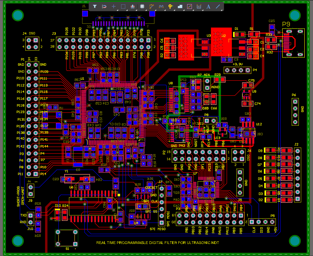
🔌 PCB Design (4-Layer)
Stack-up:
- Top Layer: Signal routing
- Inner Layer 1: Ground plane
- Inner Layer 2: Power plane
- Bottom Layer: Signal routing
Design Considerations:
- Separation of analog and digital grounds
- Controlled impedance routing for high-speed signals
- Proper decoupling and bypass capacitors
- Noise minimization for ADC/DAC paths
💡 My Contributions
- Designed complete system architecture (ADC → FPGA → DAC)
- Implemented FIR filter in Verilog
- Developed dynamic coefficient computation on STM32
- Built Python GUI for real-time user control
- Designed 4-layer PCB in Altium Designer
- Performed component placement, routing, and power planning
- Assembled and soldered hardware
- Debugged high-speed signal and communication issues
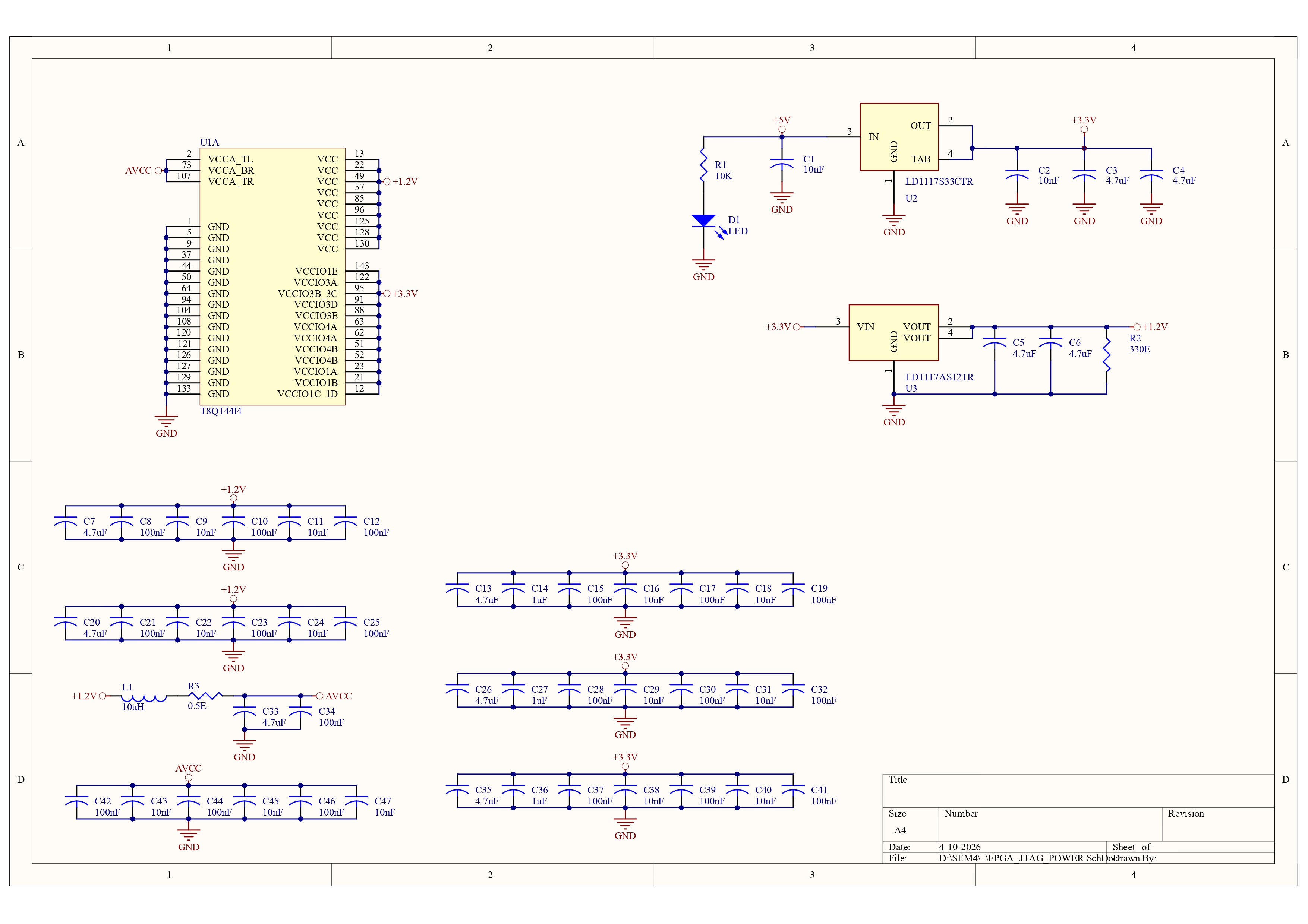
🔬 Hardware Implementation
PCB Design
schematic
 —
—
📊 Results
Signal Output

- Successful real-time ultrasonic signal filtering
- Accurate filter response for LPF, HPF, BPF
- Stable high-speed operation
- Low-noise performance due to optimized PCB design
📂 Downloads
- 📄 Schematic
- 🧾 PCB Layout
- 📦 Gerber Files
- 💻 STM32 Code
- 🔷 Verilog Code
🔗 GitHub Repository
(Add your GitHub repository link here)